

Youngjun Song, Yeshaiahu Fainmanand, Michael J. Heller
University of California San Diego, Depts. Nano Engineering/Electrical and Computer Engineering, La Jolla, CA 92093-0412
Introduction

The fabrication of hybrid flexible photovoltaic/battery devices will require integration of many different polymers and nanocomponents that have to be organized and layered in a highly controlled manner. To this end, a variety of different Layer by Layer (LBL) processes are being used to fabricate photovoltaics, batteries and fuel cell devices. This project proposal relates to the development of a unique electric field directed layer by layer (EFD-LBL) assembly process which provides major advantages for the production of flexible hybrid photovoltaic/battery devices. Single nanoparticle layers can be deposited at a rate 100-1000 times faster than by passive assembly. Thus, complex structures with a large number (>100) of total layers can be produced in minimal time. The final project goal will be to demonstrate the fabrication and lift-off of a viable flexible device of approximately 5 cm2. In addition to photovoltaic/battery devices, the EFD-LBL process has potential for fuel cells, smart materials and miniaturized biosensors.
Methods
Electric Field Directed Self-Assembly Nanoparticle Layering Process
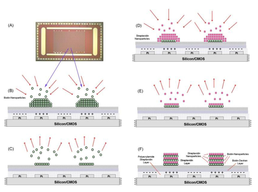
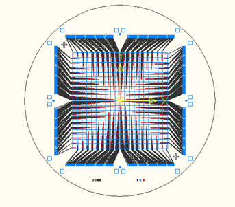
Using a 400 site CMOS microarray device and controller system we have previously demonstrated rapid and highly parallel assisted layer by layer self-assembly of biotin and streptavidin and DNA derivatized nanoparticles into higher order structures.[58,59,60] The basic scheme for the directed electric field assembly of biotin and streptavidin nanoparticles into multilayer structures on a microelectronic array device is shown in Figure 4. The 400 site CMOS microarray is shown in (a). In the initial step, positively biased test sites on the microarray attract and concentrate the negatively charged biotinylated yellow-green fluorescent nanoparticles to the surface (b). The biotinylated nanoparticles become bound to the streptavidin layer, and the unattached nanoparticles are washed away (c). (Biotin is a small biomolecule ligand which forms a strong and specific noncovalent interaction with the protein, streptavidin). In the next step, the positively biased test sites on the microarray attract and concentrate the negatively charged red fluorescent streptavidin nanoparticles which become bound to the biotinylated nanoparticle monolayer (d). The alternate addressing, binding and washing of biotin and streptavidin nanoparticles is repeated to form the multilayer nanoparticle structures (e and f).
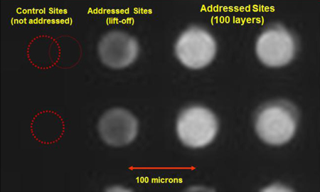 Parallel Directed Self-Assembly of 100 Alternate Layers of 40 nm Green Fluorescence Streptavidin Nanoparticles and 40 nm Red Fluorescence Biotin Nanoparticles (< one minute per addressing)
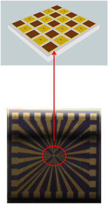
Design of New Electric Field Nanomanufacturing Array for 3D Structures, Materials and Devices
The EFD-LBL device & System
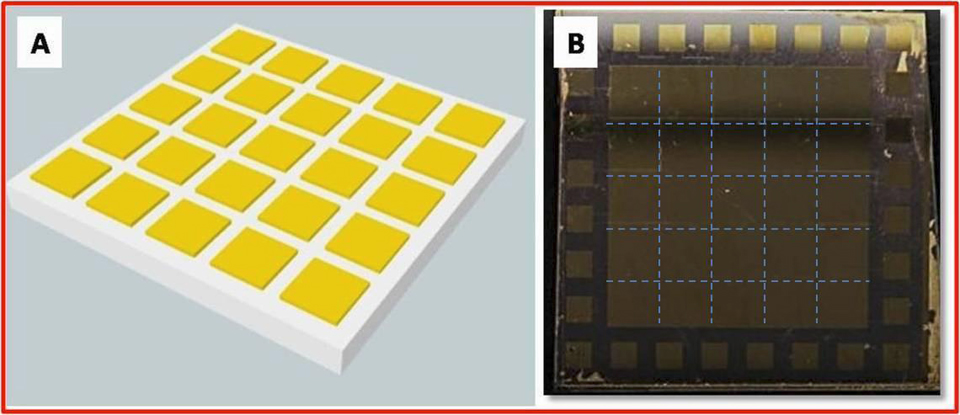
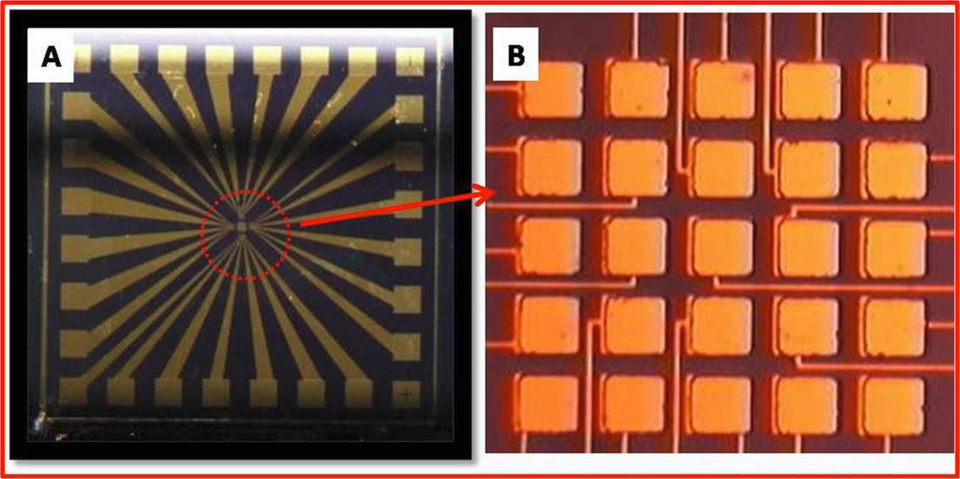
(A) shows basic design of the larger scale 5 X 5 array device. (B) shows the actual 5 by 5 array device with a matrix of 25 individual 4mm X 4mm gold microelectrodes (outlined in blue). The spacing between the microelectrodes is 30 microns. The overall array is about 3 cm X 3 cm in size, with Individual electrical contact pads for each of the electrodes on the outer perimeter.(C) shows the actual 5 by 5 array device with a matrix of 25 individual 100um X 100um gold microelectrodes. The spacing between the microelectrodes is 30 microns. The overall device is about 3 cm X 3 cm in size, the actual microelectrode array area is 500um X 500um with Individual electrical contact pads for each of the microelectrodes on the outer perimeter.
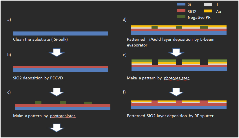
Shows the fabrication process for the microelectrode array chip which includes: a) clean the wafer b) SiO2 deposition by PECVD c) and d) patterning the Ti/Au layer, and e) and f) patterning the SiO2 layer covering wiring between the contact pads and the microelectrodes.
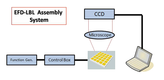
In order to control the EFD-LBL array device (regulate current and voltage), we constructed a control switch board connected with function generator (Agilent) which can apply a wide range of AC and DC voltages. The control box can independently switch voltages to the individual electrodes on the array device. A fluorescent microscope with a CCD camera is used to monitor the nanoparticle layering on the chip array device.
The system diagram with AC/DC function generator, control box and CCD fluorescent microscope.
Reagents
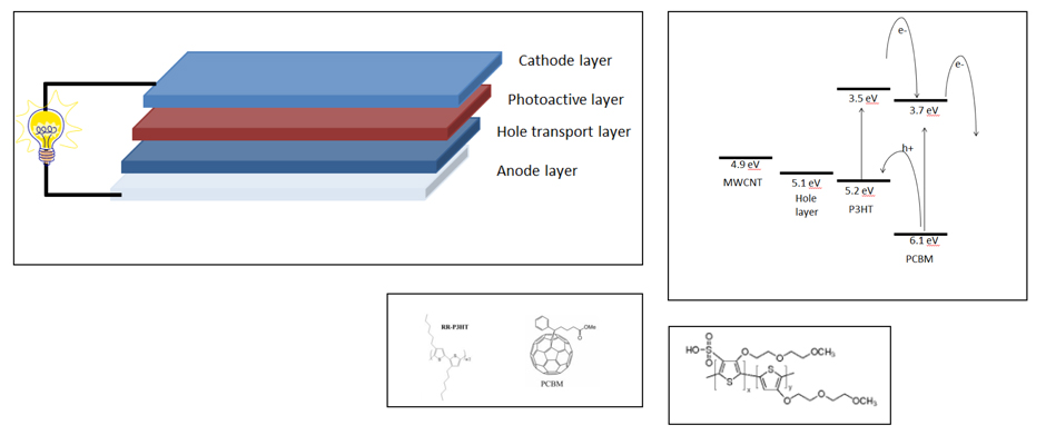
As a transparent metal layer anode, carbon nanotubes provide a good opportunity because this material is transparent, has metal characteristics, and can be charged for use in solution. In order to disperse carbon nanotubes, we dilute them in a DI water solution with polyvinylpyrrolidone (CNT: polyvinylpyrrolidone: DI water, 10:1:2000), since the CNT has hydrophobic characteristic, and dilute on the ethanol solution (CNT: Ethanol, 10:2000). CNT’s are sonicated for 90min and then centrifuge at 8000rpm.This procedure produces carbon nanotubes which have a negative zeta-potential in the DI water (1.73mS/cm, pH7.8). As a photovoltaic layer, we will use conductive polymer PCBM/P3HT mixtures (Plextronics, Inc). PCBM (Phenyl-C61-butyric acid methyl ester) which are conductive polymers combined with buckyball structures that work as n-type semiconductor (electron acceptor). The P3HT polymer works as p-type semiconductor (electron donor). This mixed material dilutes into dichlorobenzene. Poly(thiophene-3-[2-(2-methoxyethoxy)ethoxy]-2,5-diyl) which have conductivity ( 2mS/cm) work as a hole transport layer.
Results
Charged PV nanoparticles/ polymer deposition
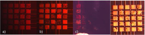
Checkerboard pattern deposition a) PV material deposition b) dry c) hole transport layer deposition d) Multi-Well carbon nanotube deposition
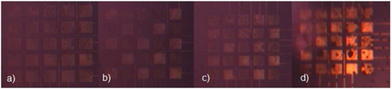
a) 0 min @DC 0V b) 1min @-2.4V c) 1min @+2.4V d) droplet polymer pouring the DI water.
Conclusions & Future Work
The Conclusion
We demonstrated the deposition of conductive polymers and nanoparticles for photovoltaic materials using our EFD-LBL device. It means after this whole layer lifts off, it is wrapped on PDMS which works for transparent, insulated and flexible cast. We think our technology, Rapid Fabrication Process for flexible and thin photovoltaic devices, works not only solar cells, but also energy martials such as battery, fuel cell. This is because we believe that the EFD-LBL process technology promises fast, cheap and robust fabrication of solar cell and battery system as well as novel small size bottom-up electronic device such as OFET, OLED, nanowire transistor or graphene device. In order to find the best conditions to optimize on EFD-LBL process, we are using charged nanomaterials and polymers which are either soluble or dispersible in aqueous solutions.
Re-Design to large array and small gap
Using the e-beam writer, Cr mask and stepper , we worked on narrowing the gap between the microelectrodes. In principle the microelectrodes are designed to be independent. But, when two more microelectrodes are in proximity to one another, the goal is to have the nanoparticle layer overlap the gap between the two microelectrodes so as to make a continuous nanoparticle layer. We believe for the larger electrodes (millimeter size range), gaps can be from 10 to 50 microns. While for microelectrodes in the 10 to 100 micron range, gaps should be in the 5 to 10 micron range. After deciding on the appropriate gap distance, we will redesign the large array chip, using the Cr mask (Photoplot Store, Inc.) and use the control large array signal using micro-control unit such as AVR.
[1] Z Liang, et al. Adv Functional Materials 16, (2006)542-548, [2] DA Dehlinger et al., SMALL V3, #7 (2007) 1237-1244, [3] DA Dehlinger et al., J Lab Automation, V12, #5 (2007) 267-276, [4] DA Dehlinger et al., NanoLetters 8, (2008) 4053-4060